EEPROM as a USB Mass Storage
by dweller - 2024-10-17
Hi there! So for a long time I was mulling over creating a computer on some old CPU like a Motorola 68000. I got some parts, namely the CPU and some random RAM and ROM chips. I even freeran it, but that’s a story for another time.
What's freerunning?
Basically, I connected all the data bus lines in such a way the CPU always reads NOP, or equivalent instruction. Then reset it and let 'er rip. CPU just goes through the whole address space, and if you connect LEDs to the address bus you get the world's most elaborate way to make a binary counter.As it happens often with me, I was distracted with something else and haven’t made progress on this endeavor. But this curse has two sides, while working on yet another project, I had an urge to tinker with hardware again. Thus I looked at my old schematics and decided that it’d be better to start with a smaller part, and finally get something physical in my hands.
Since I already had the CPU crunch through the address space, the next logical step is for it to have some code to execute. That code needs to be somewhere the CPU can fetch from. For that I got a couple of old Atmel (now Microchip) 28C256 EEPROMs. For those unaware, EEPROM stands for Electrically Erasable Programmable Read-Only Memory. Quite a mouthful. Essentially these are like Flash storage but older. Logically the next question is: how do I get code on the EEPROM?
Well, a normal person would just buy a EEPROM programmer that supports a wide variety of chips. But you, dear reader, already know that with a setup like this I didn’t do that. I decided to make my own programmer, it can’t be that hard, right? And I need practice anyways. At first I thought about doing what everyone else did, get an Atmega microcontroller write a serial protocol to transfer binary images to it and let it program the chip. But that’s boring! Besides why reinvent the wheel (did I really just said that? lol) when there’s a perfectly good serial protocol already implemented in my PC and OS. Well, okay, maybe it’s not “perfectly good” but it sure does exist, I of course am talking about Universal Serial Bus. USB has a generic device class called “Mass Storage”, so all OSes that support USB specification should support it too. You know that’s what the USB sticks use to expose Flash storage to you. Although I guess these days everyone just uses “the cloud”.
Anyways, there’s another perceived advantage to this route. I also won’t need to write a client
program that talks to the microcontroller over serial, since USB MSC (Mass Storage Class) will be
presented as a SCSI device (because really it just wraps a
subset(?) of SCSI over USB). So on Linux-based OS I will just see /dev/sd* block device which I
can just dd to/from and voilà. “UNIX is my IDE!” as
they say, or rather “UNIX is my EEPROM programmer” in this case I guess. I can also verity with like
md5sum or xxhash or something. I also decided on USB because I bought a few
Raspberry Pi RP2040-based MCUs and they have built
in USB hardware.
Now that I’ve got a plan, it was time to execute on it. First order of business was to prove it’s valid, I grabbed RP2040 micro, a couple of shift-registers (the 28C256 is a parallel chip, so I need more lines than I have on the microcontroller), a couple of level-shifters (RP2040 is a 3.3v device, while 28C256 is a 5v device), breadboard and wires, as well as PDFs for the data sheets of all the components.
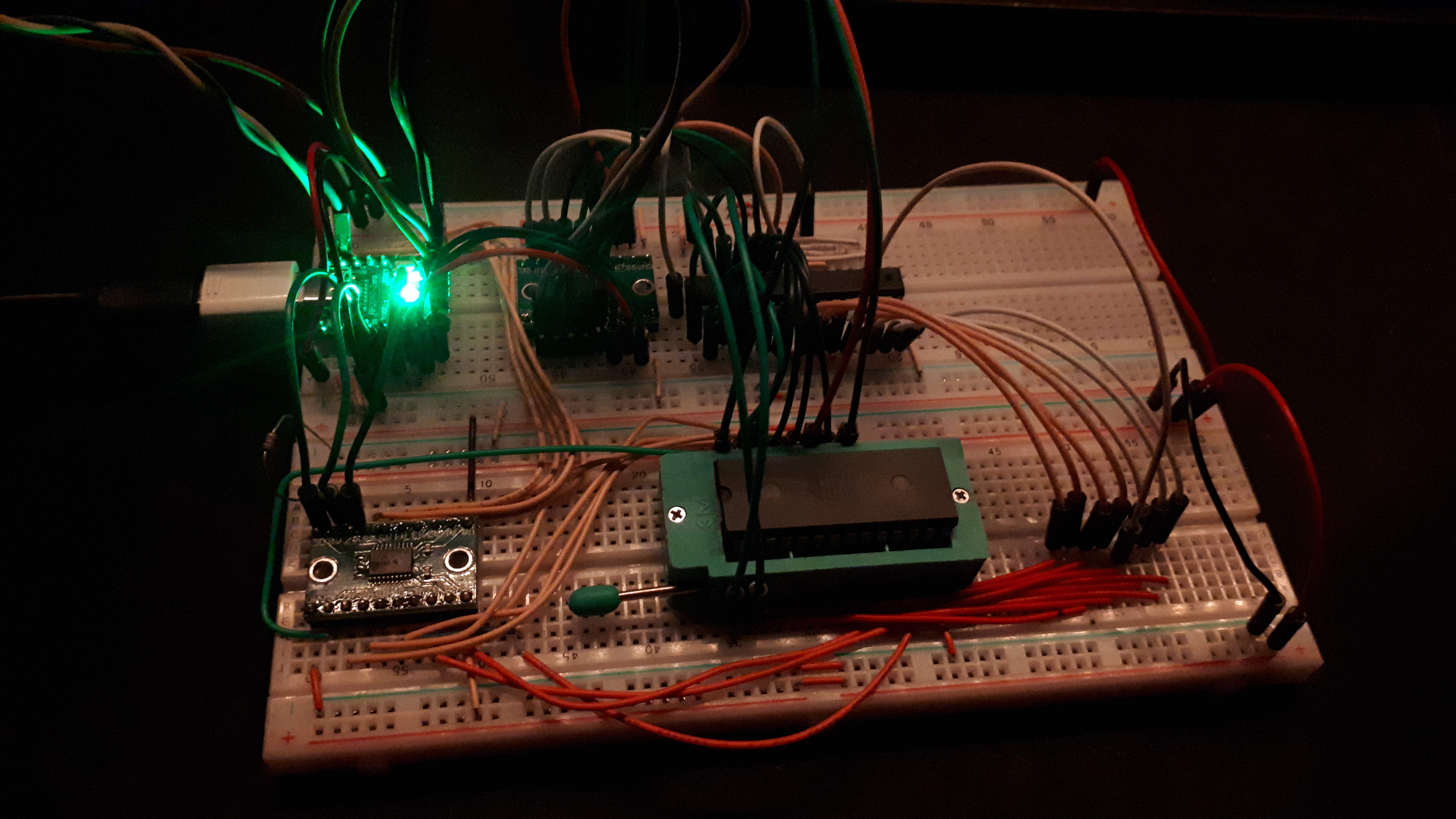
After making and fixing a bunch of bugs, cursing cmake and figuring out how to work with tinyusb again I managed to hack something that seemed to work.
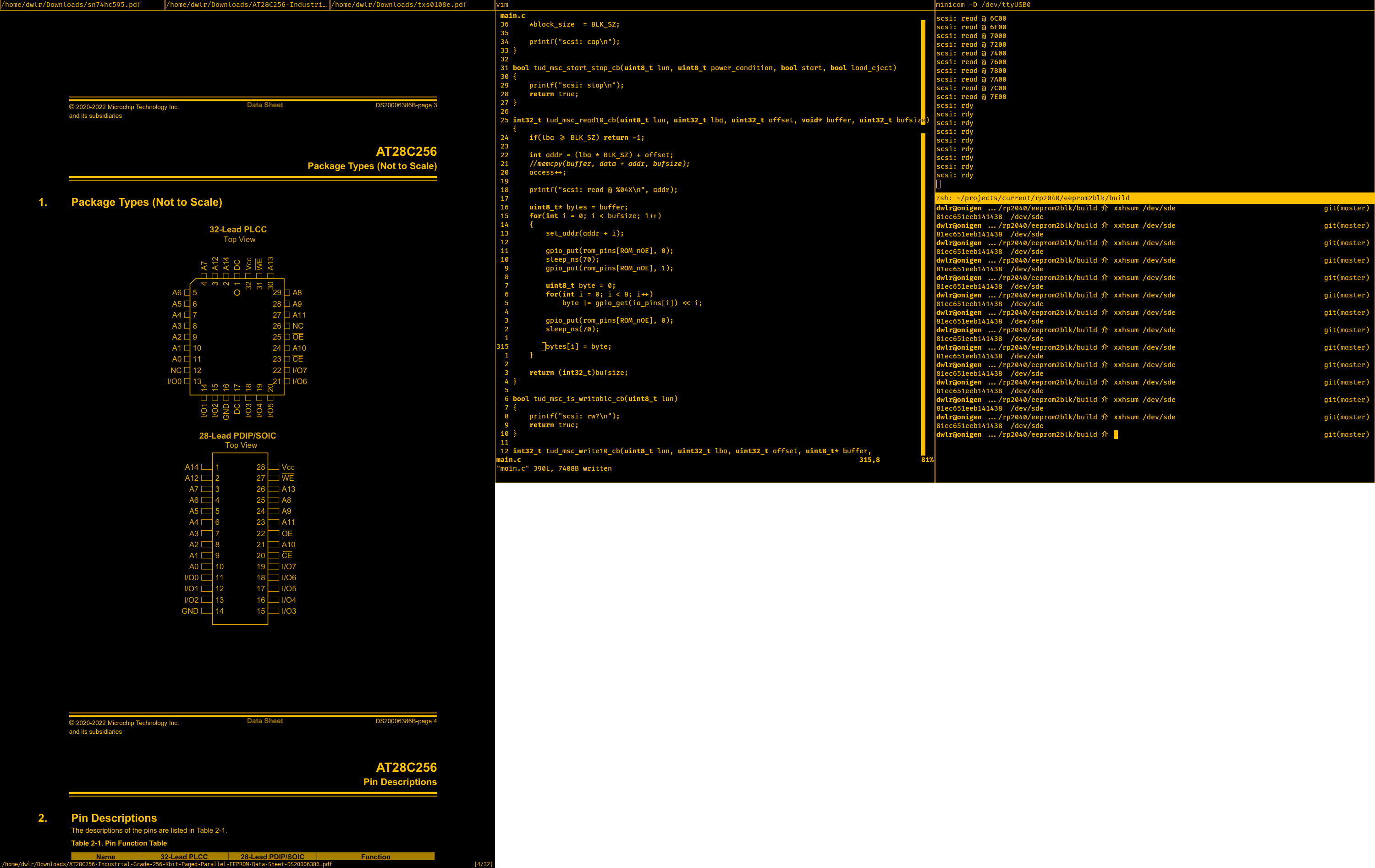
I won’t explain how it works, you can check the code if you’re interested here. Suffice it to say, I just configured tinyusb in MSC mode, and the only non-obvious thing I needed to do is to move data writing part to the other core so tinyusb could keep processing the USB packets on the main core. (Did I mention RP2040 has 2 cores? Well I did now.)
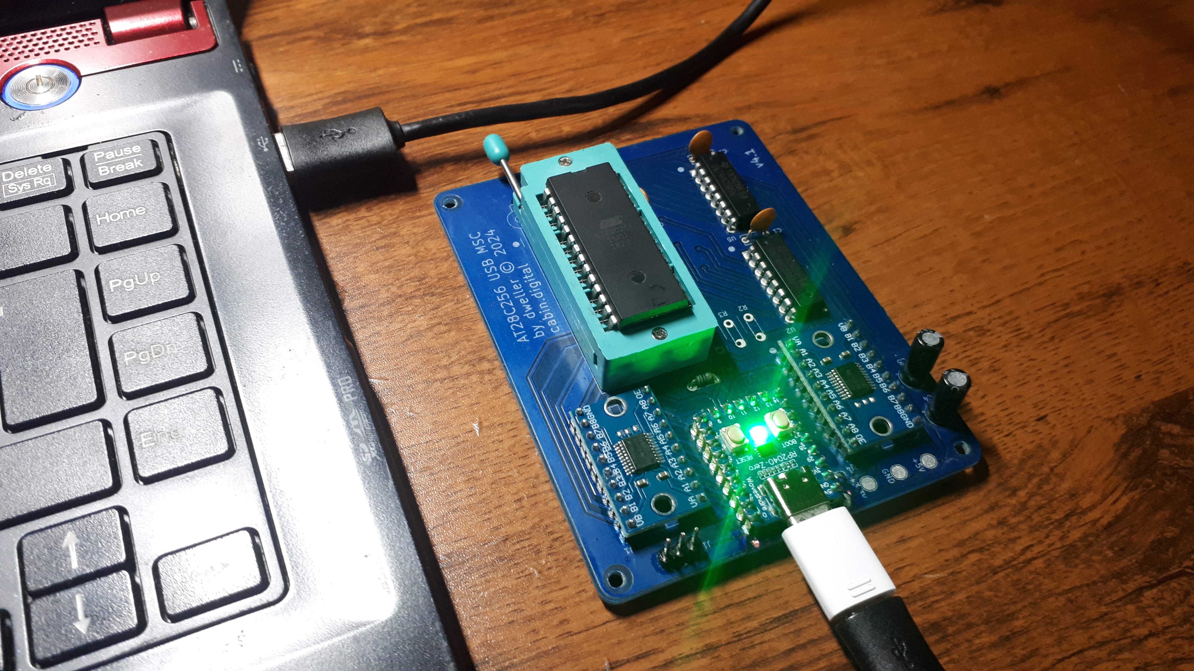
I was really happy it worked, but I really didn’t want to solder this many connections by hand, as such I decided to finally make my first Printed Circuit Board! For that I used KiCAD which I already used for schematic creation and played in the PCB layout tool once or twice. I transferred the breadboard into a schematic, and started routing the PCB.
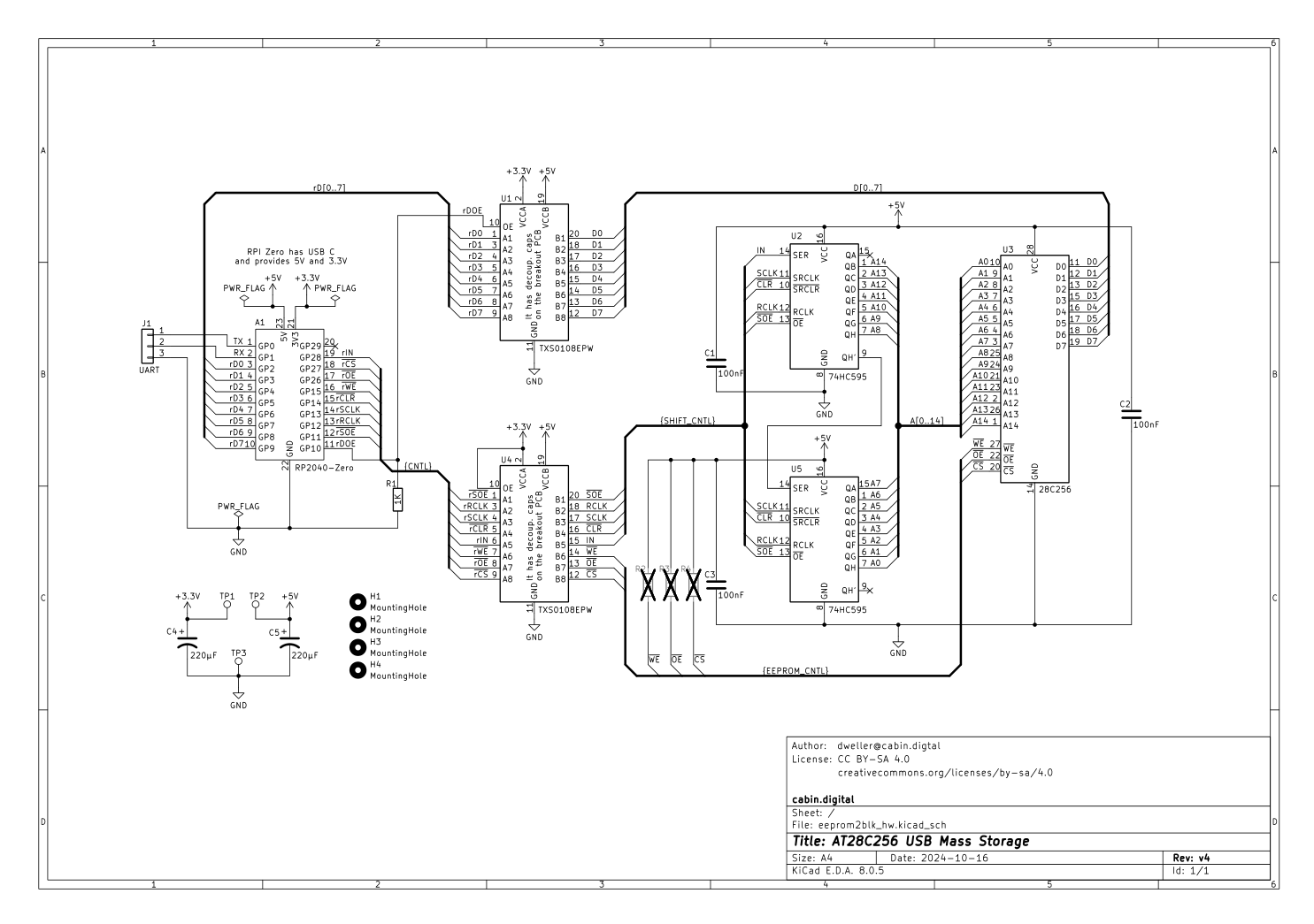
I also decided to give a local PCB manufacturer a go instead of ordering from China, since I didn’t want to wait for a long time and the shipping cost was like 4x the actual PCB cost. Also the fabs I checked out had 5 pieces minimum order, and IDK what I would do with them anyways. This limited me to a two-layer design, which isn’t a problem for something as simple as this project.
Given that this is my first time for real laying out a board I struggled a bit at first. I then remembered a simple rule for laying things out, namely the Manhattan routing. In essence it suggests using one side of the PCB for vertical tracks, and the other one for horizontal tracks. That really helped me out, since prior to remembering and realizing how useful this is I was stuck with too many options of how to route my traces and it all ended up pretty spaghetti-like.
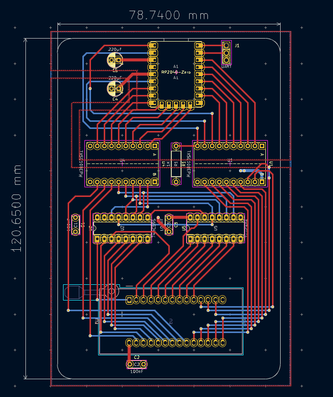
Now, as soon as I was done with the original layout, I decided that I can do better since I learned new things, and I made 4 more designs (actually 5, but that’s post-PCB shipping). After talking to a friend who actually knows Electronic Engineering I decided to ditch Manhattan layout and try to route as much as I can on the top layer to have a solid ground below it for nice return paths. Good for signal integrity and all. If you’re reading this, friend, thanks for the hints BTW! ;)
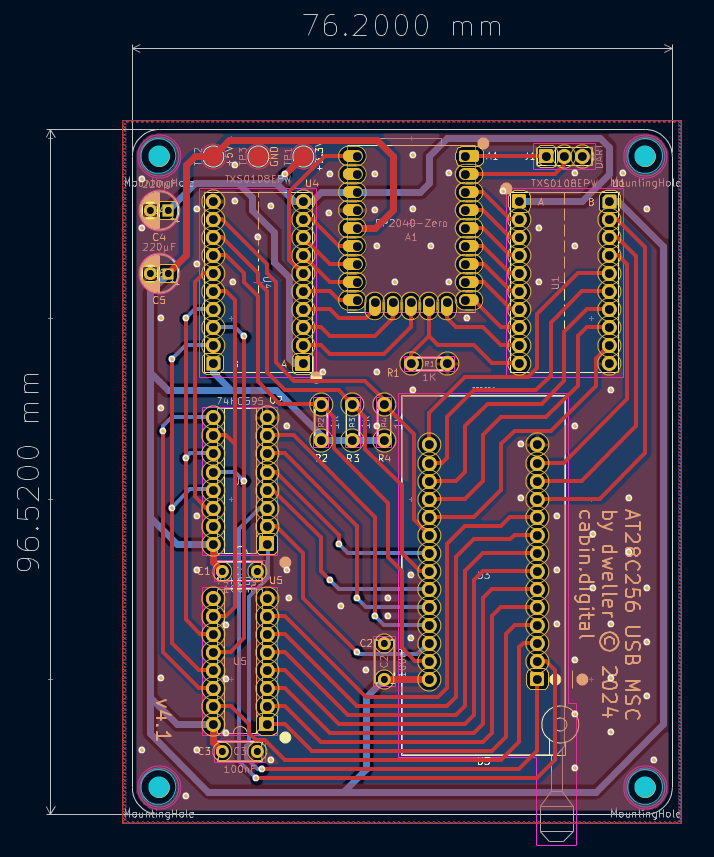
And so after 5 designs, a bunch of new knowledge and being totally unaware of what’s to come (foreshadowing too much?) I generated the gerber and drill files required for manufacturing and sent it to the fab. A few days later I picked them up and while the drill accuracy leaves me wanting I was excited to solder it up!
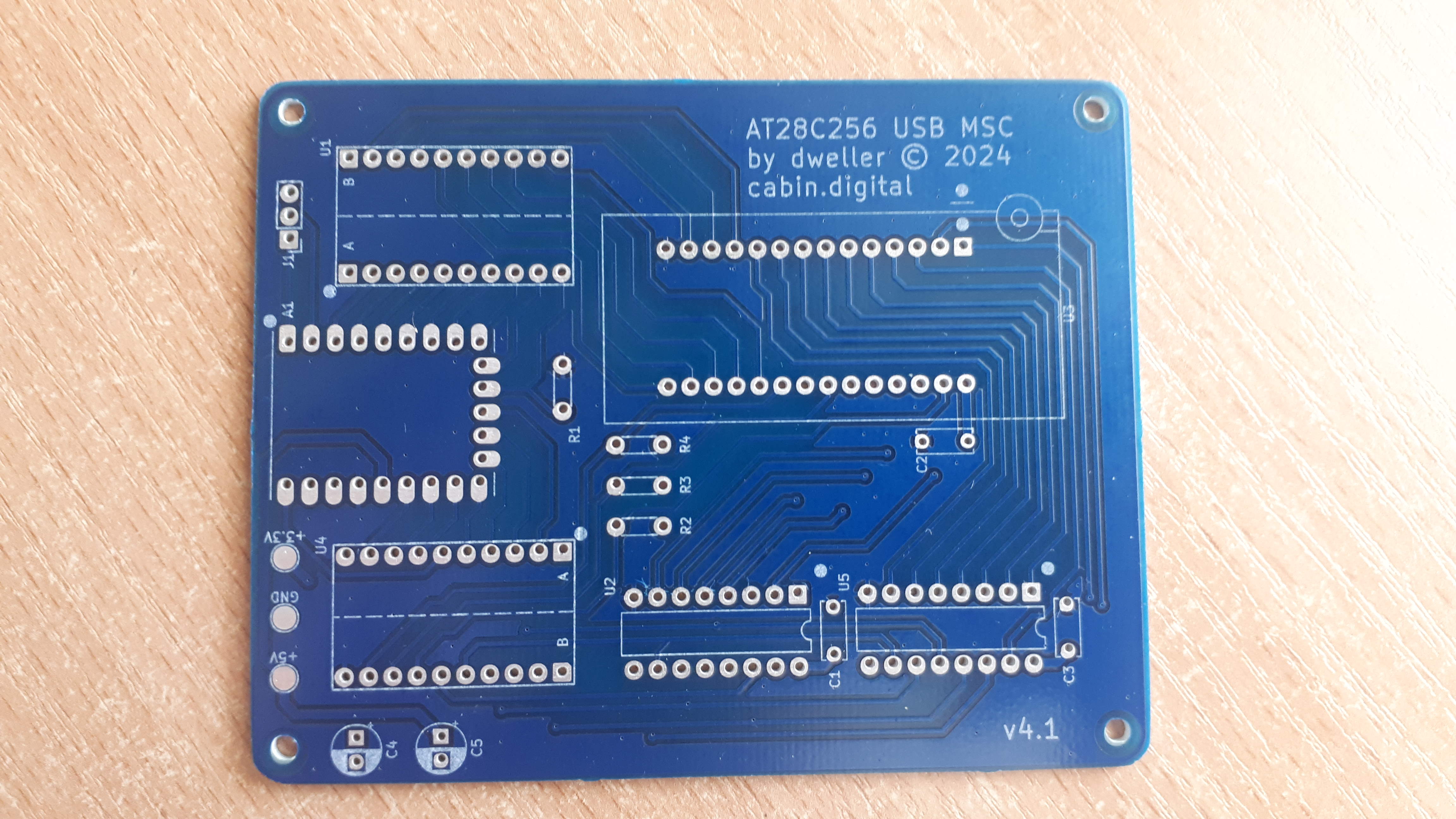
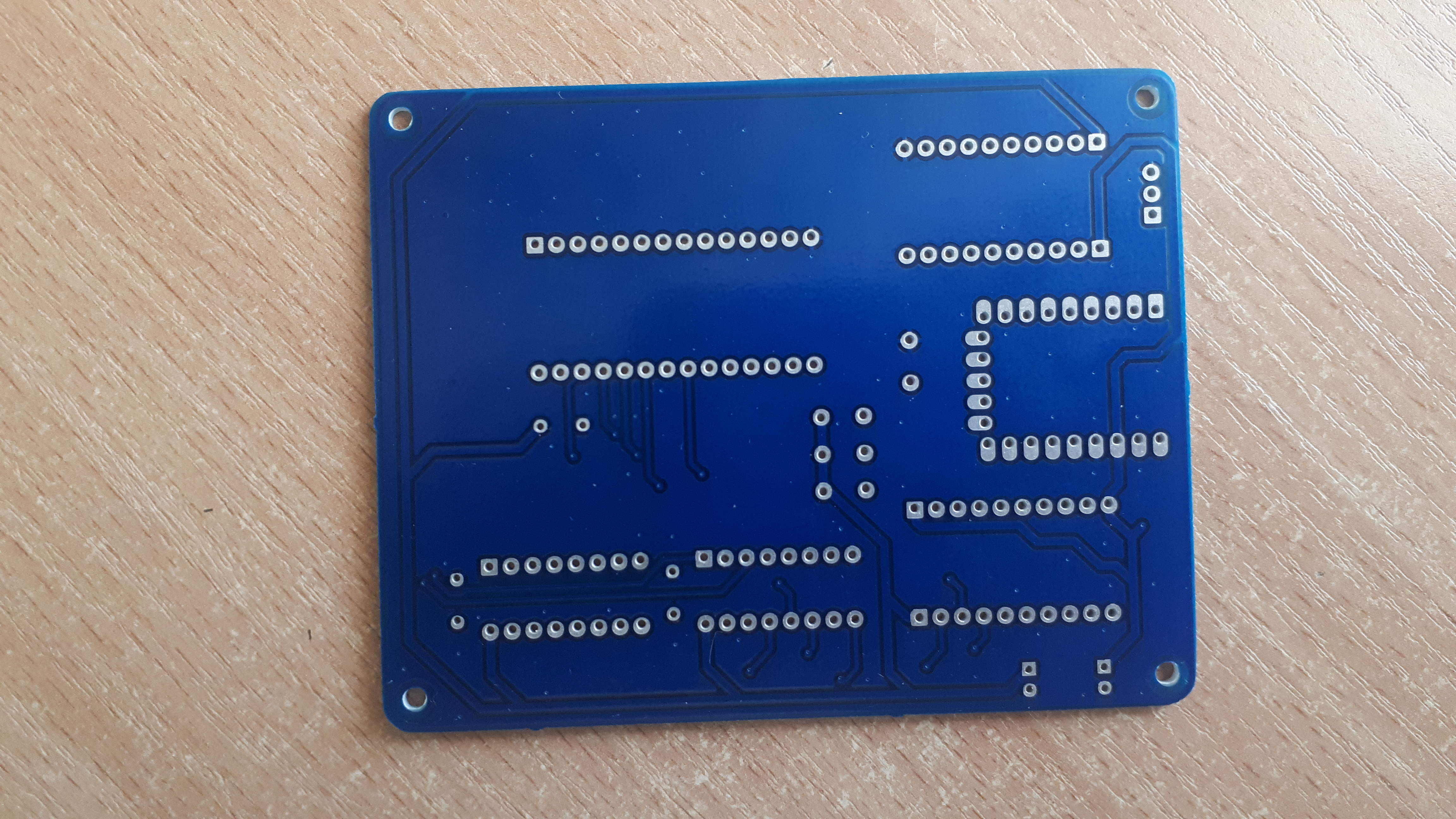
After soldering it up, I decided to test for shorts and connections with a multimeter and this is where I discovered a problem lurking in the background that I missed. You see, both the schematic and PCB have a DRC, a Design Rule Checker. It verifies if the schematic doesn’t have any obvious mistakes (like different nets(signals) shorted together) and if the PCB layout adheres to the entered fabrication tolerances, shorts, not-connected nets, etc. There’s one problem, they rely on correct input information… As you might’ve guessed, I messed something up. I reused a footprint for the RP2040 microcontroller from my usb2sun project, which only has schematics, but I decided to make footprints too even though I wasn’t going to make a PCB. Well that footprint had 5 pins vertically flipped, and they just so happened to be ground, 5 volts and a signal… You should’ve seen my face.
Well, you live you learn, you overcome. It was time to add my first PCB bodges. At first I tried to desolder the RP2040, but with my equipment I didn’t manage to. Checking my PCB layout I decided the easiest way is to cut the whole ground island beneath the micro and drill out the pin on the other side. I cut the signal pin which was connected to 5V and scrapped off the nearby trace. Ground was easy since it’s everywhere so I scraped the copper pours near the real ground pin and bridged those.
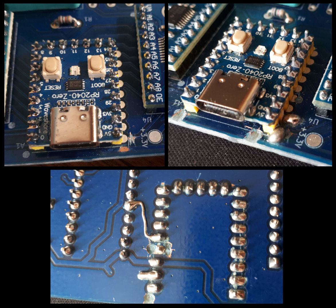
After that, it sprung to life! But as we all know, where’s a problem there’s multiple. For the life of me I couldn’t get rid of solder flux residue with my isopropyl alcohol and a brush. When washing my hands I saw that warm water and soap took the stickiness easy and fast and decided that I will try to gently wash my board with just warm water and soap. Now I know what you think, but it should be okay to do this, water on its own won’t immediately destroy electronics if they aren’t powered and if you dry them quick to prevent corrosion. But I failed to take into the consideration the buttons on the RP2040-based MCU. You see after cleaning it sometimes the MCU doesn’t start, because the reset button seems to hold it in reset… A push on it fixes that. If I am going to do more PCBs, I should probably get an ultrasound cleaner bath. I wish I didn’t learn so much from my own mistakes! :P
There is also one more thing that I can’t find an explanation to. You see after reset or power
cycle the last byte on both of my EEPROMs revert to 00. I couldn’t find anything wrong with my
code yet, and I tried adding pull ups on EEPROM’s Write Enable line (active low) but then it never
wrote. I am suspecting that my 2nd hand EEPROMs might be worn out a bit.
But hey, it works! Most of the time… xD
I could finish here, but I wanted to share another small, related story.
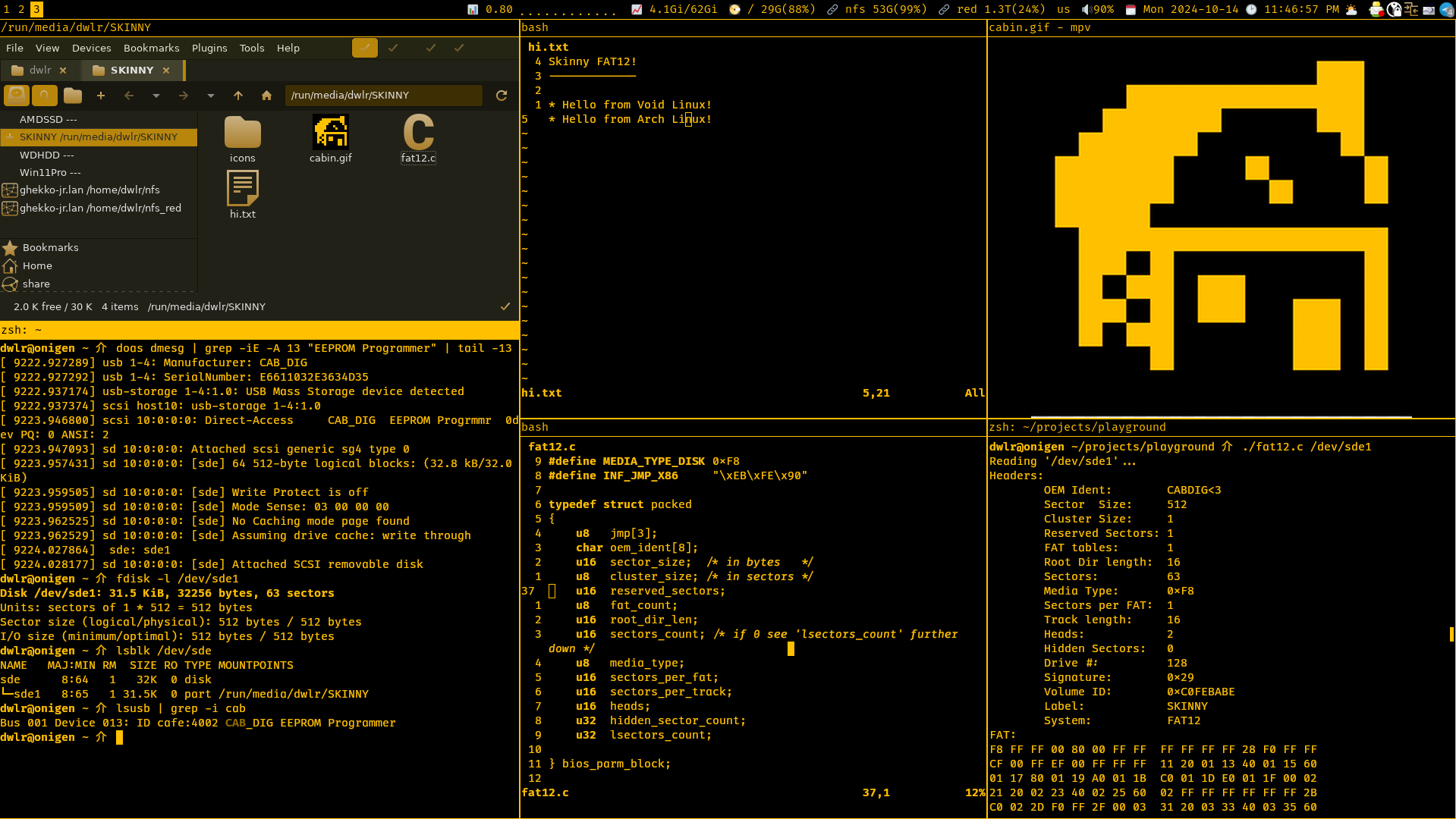
In order to test it all out, I wanted to put a FAT file system
on the EEPROM and make the world’s worst USB flash stick, but mkfs.fat refused to format it,
citing too little space. Knowing what I know about FAT, I knew you can change cluster and FAT sizes
and was sure it’s possible to fit in on the 32KB EEPROM. I hacked up a quick C program to write out
the FAT headers and sure enough. I had working file system on and old EEPROM! (I later learned that
mtools should be able to format FAT with your custom sizes
so writing it from scratch wasn’t necessary, not that it was hard. Besides I’ll need FAT support for
the m68k computer one day, right? Or maybe ext2… We’ll see, hopefully!)
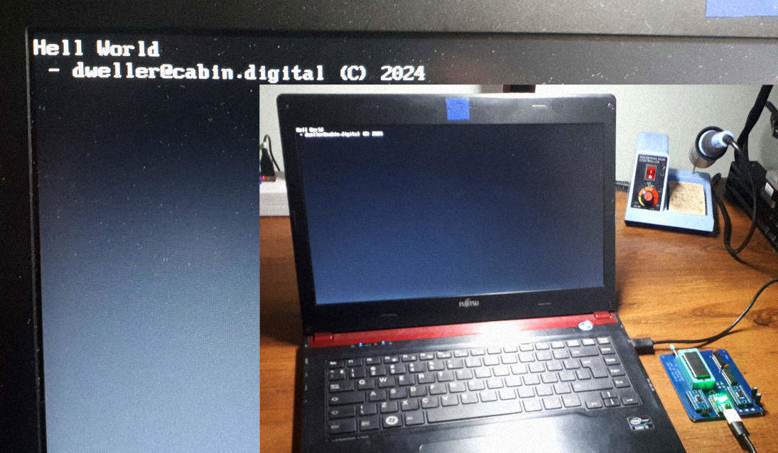
Since it’s FAT12 formatted, I figured I might as well write a quick “hello world” for UEFI and boot on it.
Anyways, I think I rambled long enough. Lessons learned, skills acquired, thing made. If you want to check the project files, they are at my git Thank you for reading all that if you got here, and do let me know if you like these more “me rambling into the ether” type of posts, or would you like more condensed and to the point posts. I am experimenting here. Oh and if you checked the project files and found a bug, feel free to tell me I am dumb too! (and why, please ;) )
More posts potentially soon, although probably not hardware related. Sometimes I wonder if I have ADHD…
dweller